Blog
-
HDI PCB making in an automated PCB factory — ENEPIG PCB surface finish
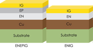
HDI PCB making in an automated PCB factory --- ENEPIG PCB surface finish Posted: Feb 03, 2023 Categories: Blogs Tags: pcb, pcba, pcb assembly, pcb manufacturing, pcb surface finish, HDI ENEPIG (E...Read more -
HDI PCB making in an automated PCB factory — OSP surface finish
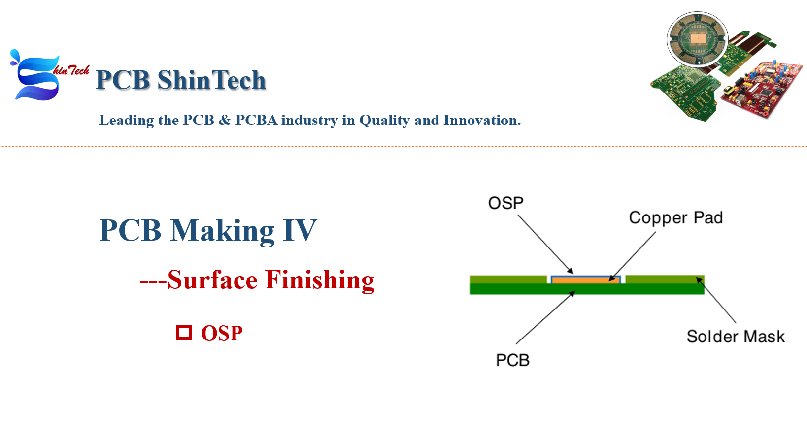
HDI PCB making in an automated PCB factory --- OSP surface finish Posted: Feb 03, 2023 Categories: Blogs Tags: pcb, pcba, pcb assembly, pcb manufacturing, pcb surface finish, HDI OSP stands for O...Read more -
HDI PCB Making —Immersion Gold surface treatment
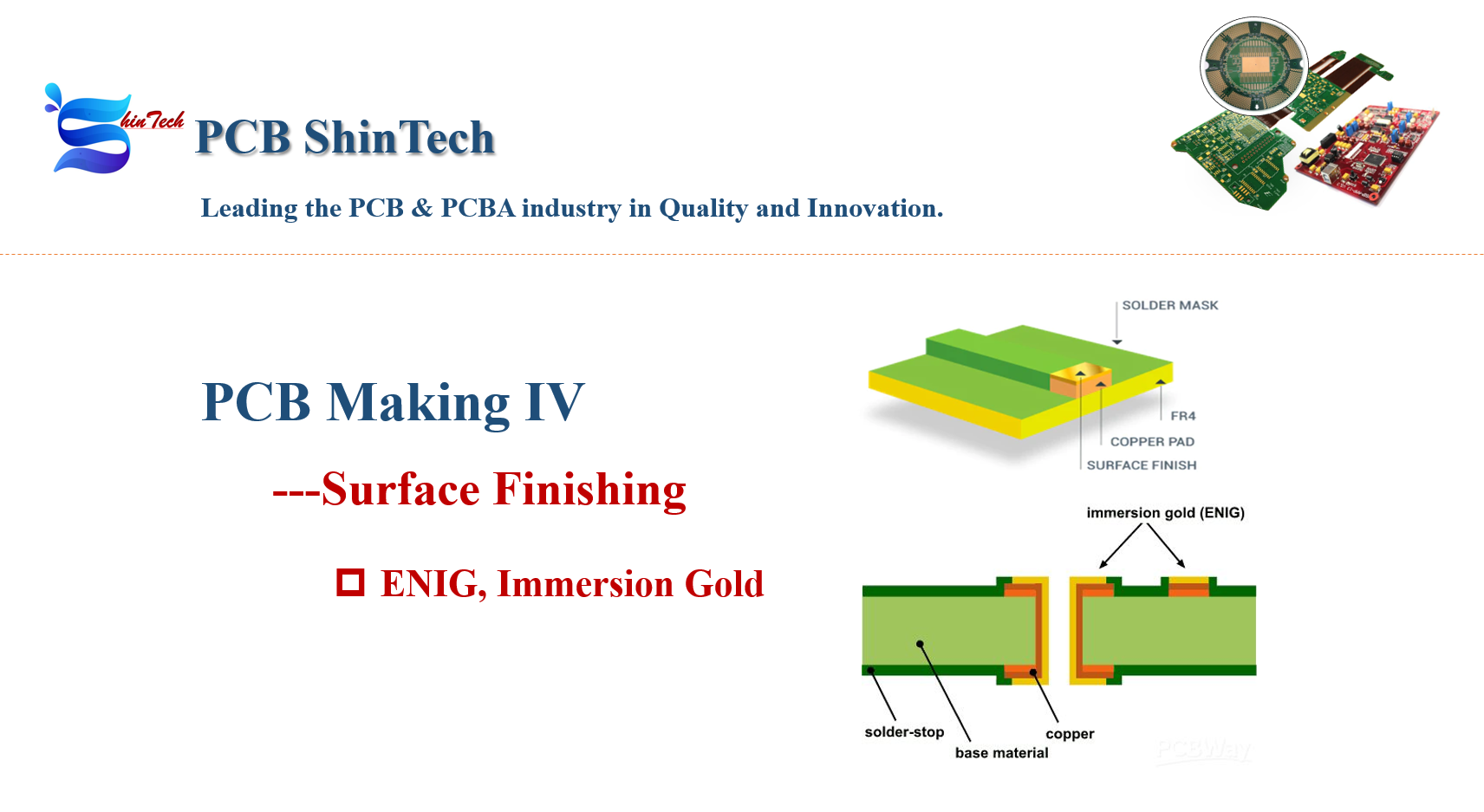
HDI PCB Making ---Immersion Gold surface treatment Posted: Jan 28, 2023 Categories: Blogs Tags: pcb, pcba, pcb assembly, pcb manufacturing, pcb surface finish ENIG refers to Electroless Nickel / ...Read more -
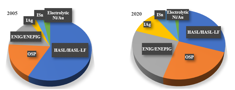
How to Choose Surface Finish for Your PCB Design Ⅱ Evaluation and Comparison
How to Choose Surface Finish for Your PCB Design Ⅱ Evaluation and Comparasion Posted: Nov 16, 2022 Categories: Blogs Tags: pcb, pcba, pcb assembly, pcb manufacturing, pcb surface finish ...Read more -
How to Choose Surface Finish for Your PCB Design Ⅲ Selection guidance and developing trends
How to Choose Surface Finish for Your PCB Design Ⅲ The selection guidance and developing trends Posted: Nov 15, 2022 Categories: Blogs Tags: pcb, pcba, pcb assembly, pcb manufacturer ...Read more -
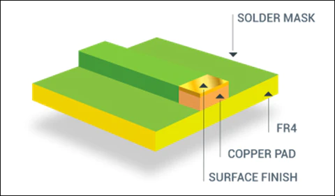
How to Choose Surface Finish for Your PCB DesignⅠ What and How
How to Choose Surface Finish for Your PCB Design ---An Expert’s Guide to PCB Surface Finishes Ⅰ What and How Posted: Nov 15, 2022 Categories: Blogs Tags: pcb, pcba, pcb assembly, p...Read more -

Multilayer PCB Fabrication—Inner layer image, develop, define, print
Multilayer PCB Inner Layer Printing Circuit Patterns are defined in a big clean and yellow room. Clean room to make sure of no dust gets onto the surface to avoid short circuits. After being clean, panels will be automatical...Read more -
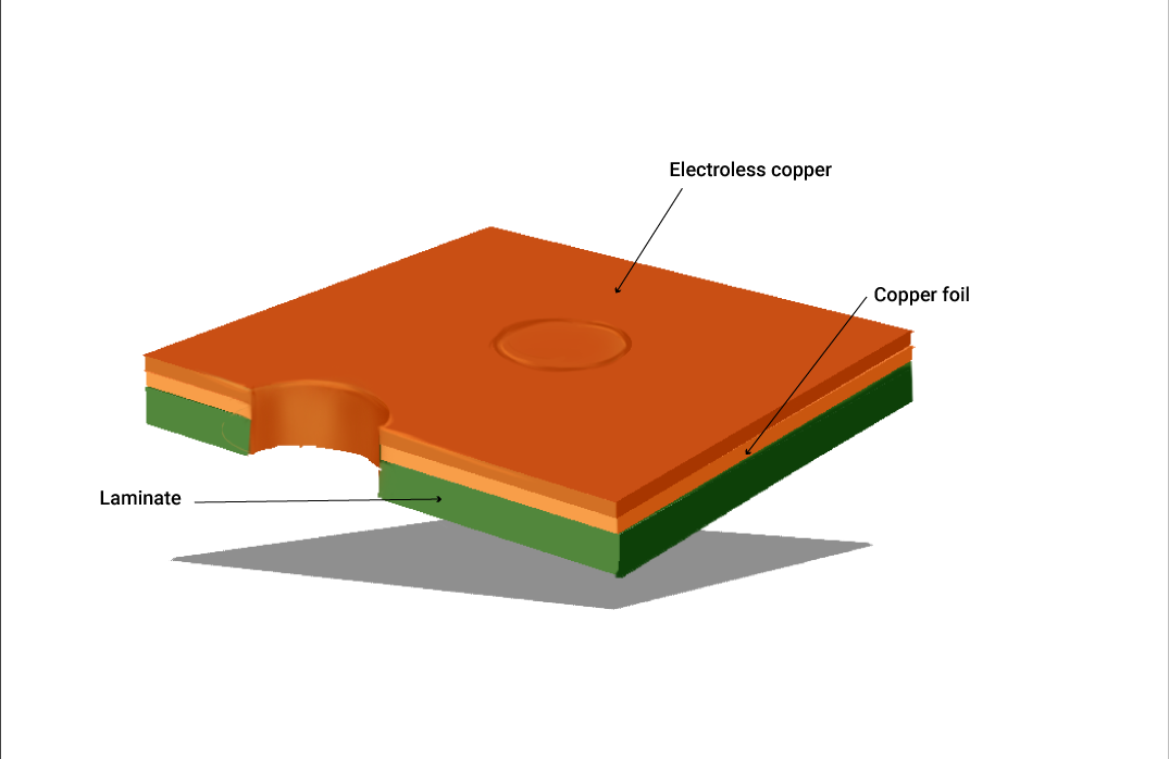
Plated Through Holes PTH Processes in the PCB factory—Electroless Chemical Copper Plating
Plated Through Holes PTH Processes in the PCB factory---Electroless Chemical Copper Plating Almost all PCBs with double layers or multi-layers use plated through holes (PTH) to connect the condu...Read more -

Laser Drilling Microvias – The Must of HDI PCB Boards Manufacturing
Laser Drilling Technology- The Must of HDI PCB Boards Manufacturing Posted: Jul 7, 2022 Categories: Blogs Tags: PCB, PCB Fabrication, Advanced PCB, HDI PCB Microvias are also called blind via-ho...Read more -
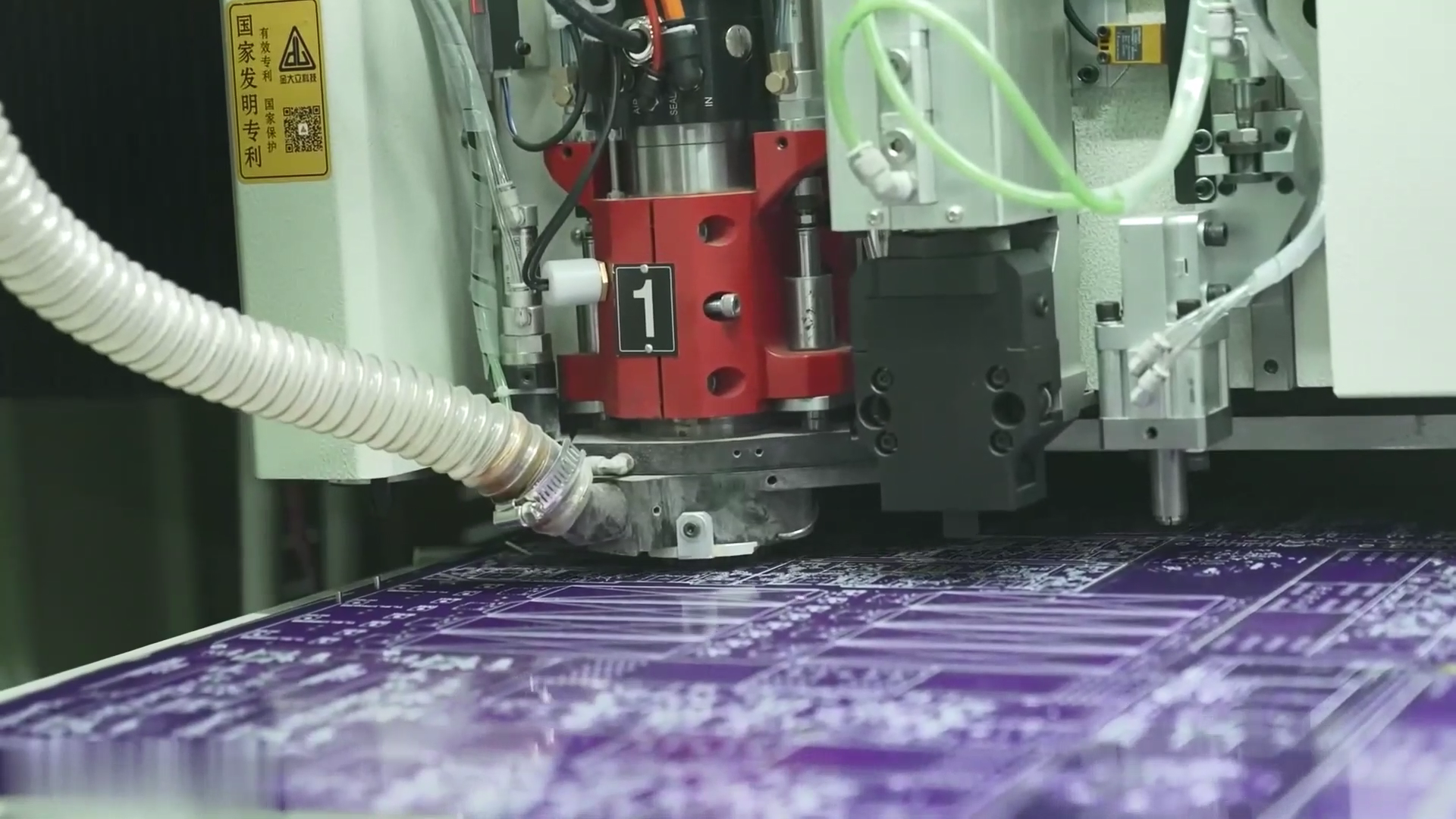
PCBs Mechanical processing
PCB Making --- Mechanical Process Posted: Jul 3, 2022 Categories: Blogs Tags: pcb, pcba, pcb assembly, pcb manufacturer One of the final operations in the manufacturing process of PCBs is mechanical processing...Read more -
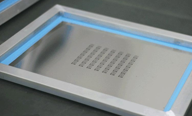
WHAT IS A PCB STENCIL AND HOW TO USE IT?
Posted: Feb 15, 2022 Categories: Blogs Tags: pcb, pcbs, pcba, pcb assembly, smt, stencil What is a PCB Stencil? PCB Stencil, also known as Steel mesh, is a sheet of stai nless steel with laser cut openings used to transfer an accurate amount of solder paste to an accurate designated position o...Read more -
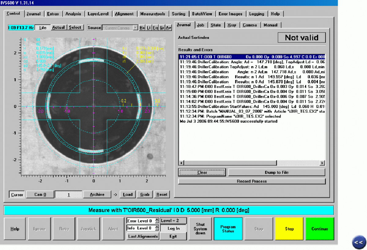
Accurate Drilling with CCD
Posted: May 26, 2021 Categories: Blogs Tags: pcb, pcbs, pcb making, pcb manufacturing, pcb fabrication, innovation, drilling, ccd As the PCB manufacture technologies improving, printed circuit boards tend to be with smaller vias and an increasing number of layers. Usually, each layer of multil...Read more